Beyond Silicon: The Potential of Nanostructures in Up-and-Coming Materials
By Cullen Walsh
The Magic of Silicon
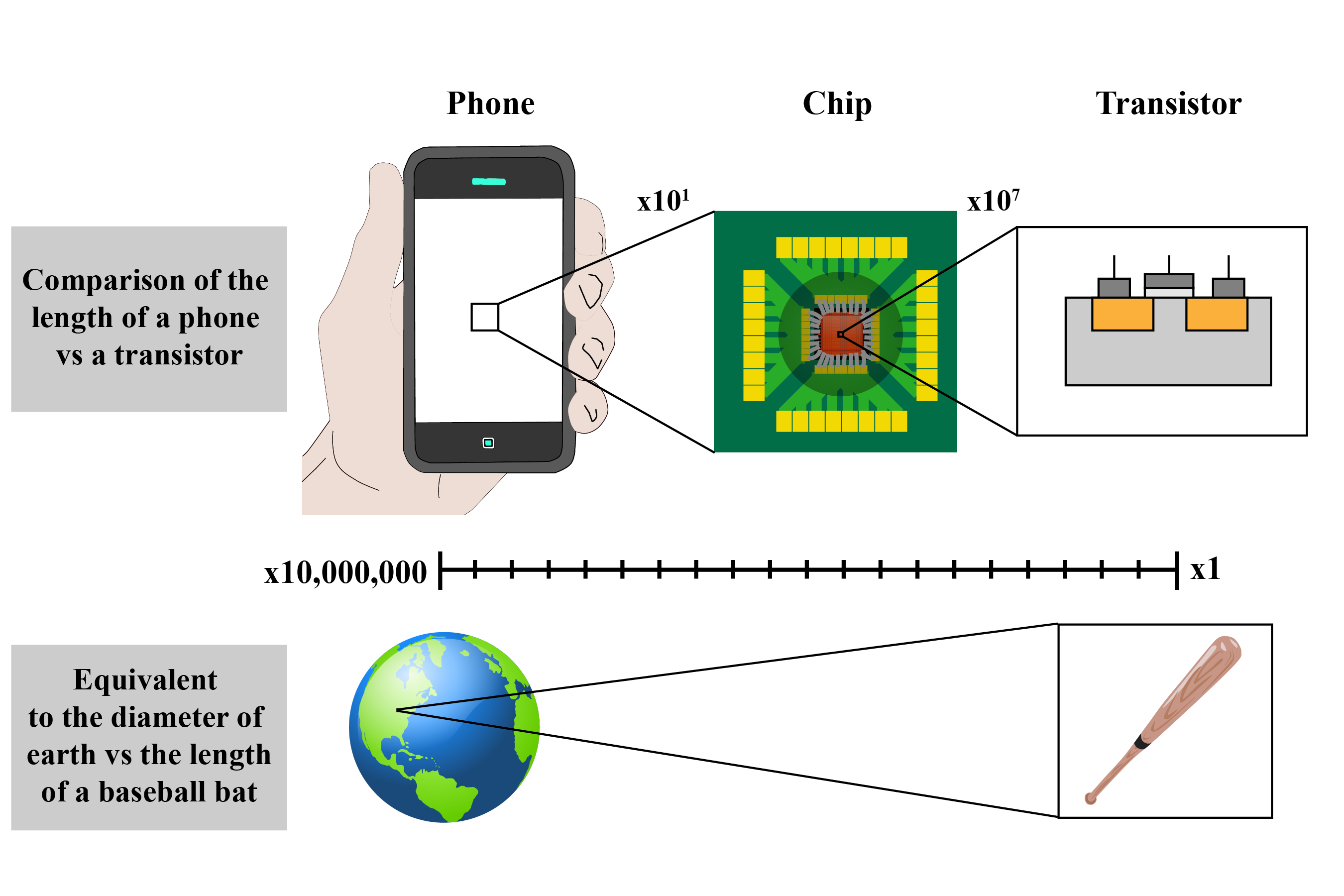
You are probably reading this article on a phone or a computer. What makes that possible is a small piece of silicon, probably a few centimeters in size, with billions of tiny on/off switches on its surface. To fit all of those tiny on-off switches, which we call transistors, onto that small piece of silicon, they need to be made at the nanoscale. As a result, the length of an average transistor is around 1/10,000 the width of a human hair. For comparison, the length of a transistor relative to the length of your phone is equivalent to the length of a baseball bat versus the diameter of planet earth.
These incredibly tiny transistors are typically made from silicon and for them to work properly that silicon needs to be made nearly perfect since even nanoscale defects in the material can be catastrophic to the transistor’s performance. As a result, researchers have refined the production of silicon to the point where we can create giant silicon crystals that are over 99.9999999% pure (what is known as the 9N level) and nearly perfectly uniform. Our ability to produce these large, highly purified silicon crystals at an industrial scale has helped drive the constant improvements in the performance of our devices.
The problem is silicon is not ideal for all use cases. For instance, it struggles to operate at high voltages, as is the case in electric vehicles. Scientists have therefore been investigating new materials that can surpass silicon in both new and established technologies. My research explores two of these up-and-coming classes of materials – layered materials and perovskites. Part of what makes these materials unique is that, unlike in commercial silicon, introducing nanoscale structures and defects into these materials can actually be beneficial, and can even lead to new material properties. However, it is not yet clear how each nanostructure, such as an edge or a tear in the material, contributes to these changes. To better understand this, I use a technique called optical pump-probe microscopy to isolate individual structures and measure how they change the optical and electronic properties. These findings could help us architect a whole new world of materials that surpass silicon in many applications and that even facilitate new technologies that do not yet exist!
The World Beyond Silicon
The two up-and-coming classes of materials that I study are layered materials and perovskites:
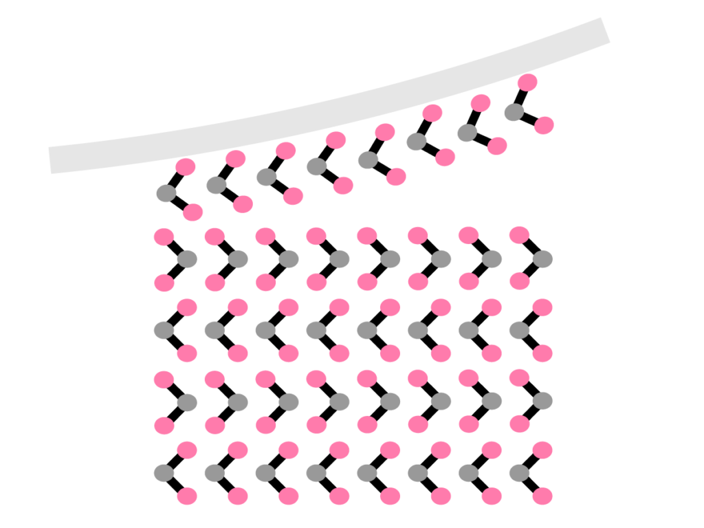
Layered materials are made up of sheets of atoms that have strong interactions within each sheet but weak interactions between sheets. Think of them like a stack of sticky notes where there is a small adhesive force holding the individual sheets of paper together. As a result, we can easily peel off individual layers using the force provided by just a piece of tape. The most recognizable of these materials is graphene, the one-atom thick analog of graphite. The problem with graphene is that it is a semimetal and is therefore of limited use in many electronic components in which semiconductors are necessary. My work instead focuses on transition metal dichalcogenides (TMDCs) which possess many of the same structural benefits as graphene but are semiconductors, making them useful in photonics and electronics applications.
I also study perovskites, an up-and-coming solar cell material that is both solution- and gas-processable, making it a potentially cheaper and more scalable alternative to silicon for use in solar energy conversion.
The Pros and Cons of Defects
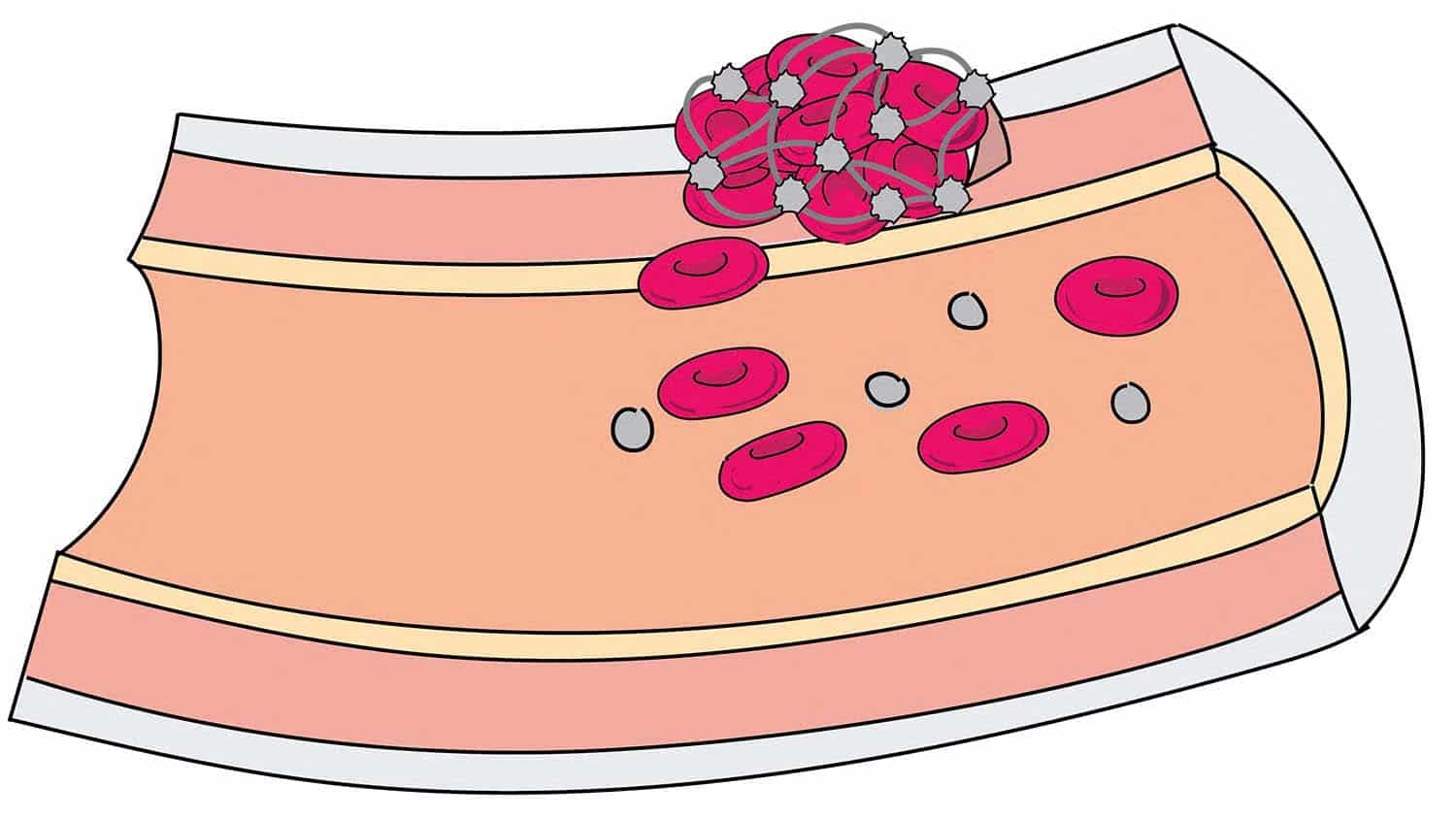
When we think about materials like silicon, the goal is typically to produce a crystal that is as perfect and homogenous as possible since this typically enhances its performance in devices. However, as researchers have explored new materials, they’ve discovered that perfection is not always ideal and that structural features can have benign, or even beneficial, qualities. For instance, the edges of TMDC nanoflakes can catalyze the hydrogen reduction reaction, an important step in hydrogen fuel production. In contrast, the defect-free regions of the material cannot.
This means that by simply adding or subtracting structural defects from a material, we can create new material properties. The problem is researchers have found that different nanoscale structures change the properties of a material in often unexpected ways. We therefore need to build a comprehensive understanding of how different structures affect a material’s properties (what we call a material’s structure-function relationship). Through my research, I study how different nano- and micro-scale structures change, and even create new, material properties in both TMDCs and perovskites.
Studying Nanostructures
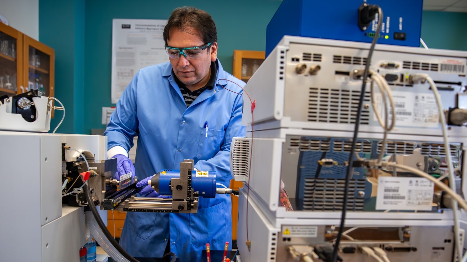
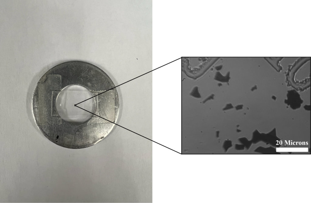
To study these nano- and micro-scale structures, I need to use exceptionally precise measurement techniques. Above is a picture of a glass slide mounted on a washer with a TMDC sample on the surface. When looking at the sample with the naked eye, it looks like there is nothing on the glass slide. It is not until we zoom in 1000x that we can see the nanoflakes clearly. To study these flakes, my research group has developed an experimental technique that uses focused laser beams to isolate the individual structures on each of these flakes and observe changes in their optical properties in both time and space.
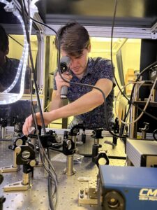
Given how precise these measurements need to be, our experiments need to be isolated from external vibrations, such as people walking around and cars driving outside. To do this, my group built our experimental setup on a laser table that floats above the floor via compressed air. On top of the table are numerous optics and mirrors that we use to manipulate and guide the laser light. Those optics send the laser light from one end of the table, where the laser is located, to the other end where we place our samples.
To get the laser beam from one side of the table to the other requires many fine-tuned alignments of the mirrors and optical components. My experiments require laser beams in the near infrared, making the beams nearly invisible to the human eye. I therefore use an infrared viewer to look at the laser beams and adjust their paths. Once all the components are aligned, experiments can begin.
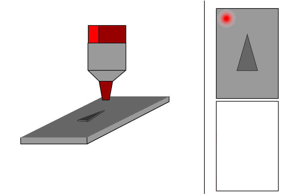
The specific experimental technique that my group has developed is called pump-probe microscopy. It involves two laser beams – a pump and a probe – that are focused to less than a micron in size (less than 0.00004 square inches). The pump beam excites the sample, injecting electrons from the valence band into the conduction band. This causes changes in the transmissivity of the material which is detected via the transmission of the probe beam. We mainly perform two different types of experiments:
This information is then used to determine how different structures change the rate at which electrons relax and diffuse through the material.
What’s Next?
Through my research, I want to show people that material synthesis and design should be more nuanced than just trying to create increasingly perfect materials. Historically, when people think of structure in materials, they often think of it as something that needs to be removed or avoided. However, structure and defects can actually be beneficial. By developing a more comprehensive understanding of the role different structural features play in a material, we can more effectively integrate them into new and improved devices. This could one day allow us to improve upon silicon in certain applications and even create the next generation of devices that change our world.
Cullen Walsh is a Ph.D. student at The University of North Carolina at Chapel Hill studying physical chemistry. He is a 2022-23 NC Space Grant Graduate Research Fellow. Walsh will be presenting his research at the 2023 NC Space Symposium.
☽
This post was originally published in North Carolina Space Grant.